 English
 中文
中文
News
-
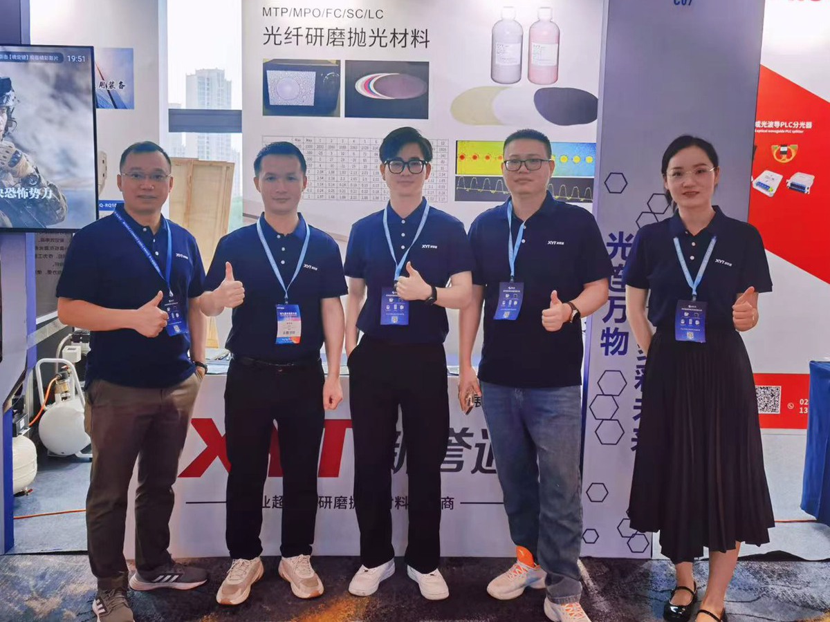
XinYuTong participated in ECOC Optical Communication Exhibition in Sweden in 2017
Products on display: Xinyutong optical fiber grinding paper, polishing belt, grinding belt and other ultra-precision grinding and polishing materials.
-
-
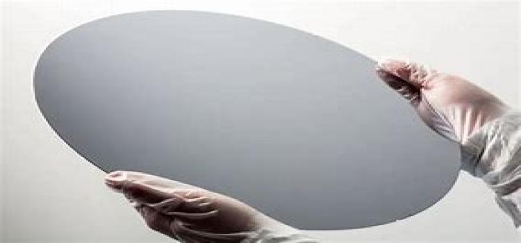
The cornerstone of chip manufacturing - semiconductor wafer industry overview
Semiconductor silicon is the semiconductor material with the highest cost ratio and the most critical semiconductor material in the industrial chain. From the perspective of cost ratio, silicon chips accounted for 37% of the market in semiconductor materials, making it the largest semiconductor material. From the perspective of the industrial chain position, silicon wafers, as the starting point of the semiconductor industry chain, directly affect the manufacturing quality of chips. This paper mainly introduces the core semiconductor material silicon wafer and its industry situation in detail.
-

-
Mirror polishing technology, too complete!
Mold polishing usually uses oilstone strips, wool wheels, sandpaper, etc., to cause plastic deformation on the surface of the material and remove the protruding parts of the workpiece surface to a smooth surface. It is generally operated manually.
-
-
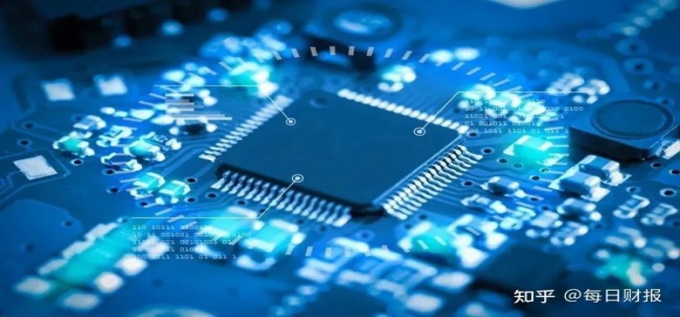
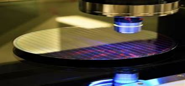
CMP for semiconductor devices
The wafer manufacturing process consists of seven independent processes: lithography, etching, film growth, diffusion, ion implantation, chemical-mechanical polishing, and metallization. As one of the key process processes of wafer manufacturing, chemical mechanical polishing (CMP) refers to the efficient removal of excess materials on the wafer surface and the global nano level flattening through the cooperative action of chemical corrosion and mechanical grinding.
-
-
Advantages, technical difficulties and realizable areas of micro-LED
Despite the rapid development of solid-state lighting, display backlighting is still a substantial market for leds. For more than a decade, screens have been displayed by these devices initially placed in traditional packages, and more recently in chip-level packages, and they are now the backlight for LCDS.